
Top chipmakers embrace ASML’s $400M machines, agree to crucial chipmaking change
Chipmaking changes could boost productivity of new ASML machines by 40 percent.
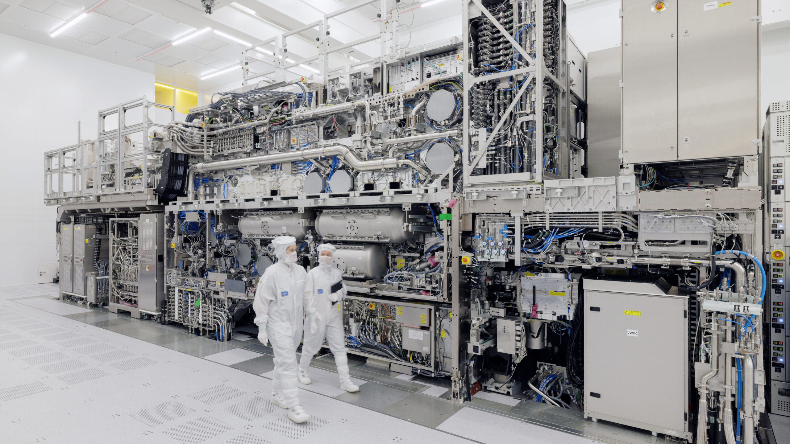
Chipmaking changes could boost productivity of new ASML machines by 40 percent.
The short version
- This signifies the semiconductor industry’s broader embrace of high NA EUV photolithography technology that can cost up to $400 million per machine and is only provided by the Dutch technology company ASML, Bloomberg reports .
- The technology would allow chip designers to implement even smaller features in potentially more powerful and efficient next-generation chips produced for AI data centers and consumer electronics such as smartphones, tablets, and laptops.
- ASML’s EUV (extreme ultraviolet) lithography machines enable chipmakers to use powerful laser light to imprint patterns in silicon wafers, layer by layer, and gradually form the computer circuitry that makes silicon chips work.
What happened
Compared to older deep ultraviolet lithography, EUV technology harnesses a more powerful source of light with a shorter wavelength to create even smaller features on silicon wafers. South Korea’s Samsung plans to use ASML’s high NA EUV machines in producing memory chips by 2028.
Why it matters
Meanwhile, Taiwan’s TSMC aims to use the technology for manufacturing the most advanced chips for its customers—including companies like AMD, Apple, Nvidia, and Qualcomm—starting in 2030.
Summary by Nerd News Network. Read the full article at Ars Technica via the links above and below.